Release the kraken!
The first version of the hvps-x aptly named “Release the Kraken” is now available. It’s time to awaken the high-voltage monster and make some sparks! All information relative to the high voltage power supply’s hardware is located on this page.
Table of contents

PCB schematic
Here is the schematic of the hvps-x electrical circuit:

PCB details
The information you need to order your boards. We recommend either PCBWay or JLC PCBs for prototypes, as they have interesting price for small quantities (USD 2 for 5 boards with JLC PCB). Sadly, the price will be dominated by shipping costs. You usually get your boards in less than 2 weeks (and half of this time is shipping).
- Size: 100 mm x 68 mm
- Layers: 2
- Thickness: 1.6 mm (recommended)
- Material: FR4 (recommended)
- Min trace width: 0.2 mm
- Min hole diameter: 0.35 mm
PCB assembly (PCBA)
Voltage rating
You can assemble your hvps-x with any EMCO series G DC-DC converters. There are different G models that can deliver high voltage up to a specific value (between 100V and 6000V). The maximum voltage requirement of your application will dictate which converter you choose.
There are a few components for the voltage monitoring circuit that depend on the voltage rating of your hvps-x. This is indicated on the bill of materials (BOM), but here is a table of the voltage-dependent components. Once you have decided which DC-DC converters you will use, make sure to use the correct values for these 2 resistors:
| Component | 6kV | 5 kV | 4 kV | Other ratings |
|---|---|---|---|---|
| EMG1 | G60 | G50 | G40 | Contact us |
| R7 | 52.3 kΩ | 64.9 kΩ | 80.6 kΩ | Contact us |
| R14 | 261 kΩ | 316 kΩ | 392 kΩ | Contact us |
We have only calculated (and tested) values for 6kV, 5kV, and 4kV EMCO series G DC-DC converter. We can provide values for other ratings, but we wouldn’t recommend the hvps-x topology for voltages below 3kV, as other approaches with cheaper components are better suited at lower voltages.
Hardware Assembly
To assemble a PCB, follow the hardware assembly, testing, and calibration instructions below step by step:
- Assembly of the SMD/SMT components
- Testing communication with the micro-controller
- Assembly of the low-voltage through-hole components
- Testing the low voltage components
- Assembly of the high-voltage components
- Testing of the high-voltage components and potting
- Calibrate the high-voltage power supply
- Print a protection enclosure
Hardware description
Hardware in a nutshell
A high-voltage DC-DC converter produces a continuous, user-controllable voltage between 0 V and the maximum output of the DC-DC converter (this can be chosen during the assembly of the board; typically 4-6 kV). A high voltage switch that can rapidly turn on and off is placed between the high voltage DC-DC converter and the high-voltage terminal output. The output of the power supply can thus rapidly change between 0 V and a user-defined voltage. The state of the switch can be manually controlled via the GUI or a physical push-button, or it can be set to switch automatically at a user-defined frequency, leading to a square wave voltage output.
In the future, we plan to provide the option for a bipolar voltage output (between -HV and +HV). Currently, only the unipolar configuration (output voltage between 0 and +HV) is available.
Main functional hardware components

- Input barrel Jack: This is the main input power of the circuit. You need a +12V DC power supply with a positive centre 2.2 mm inner diameter and 5.5 outer diameter barrel plug. One possible solution is XP Power VER12US120-JA
- High Voltage safety switch: This mechanical hardware switch controls the power to the high-voltage components. When it is on position 0, there can be no high-voltage at the output of the hvps-x, irrespective of any software / firmware settings (or bugs!). This switch should always be placed on 0 when the unit is not used, and — most importantly — when touching the high-voltage cable (for example when connecting a device under test).
- Buck converter: The PWM-controlled buck converter can produce a voltage between 0 and 12 volts. The PWM control signal can take 1000 different values.
- XP Power (EMCO) series G DC/DC converter: hvps-x is designed around the XP Power (EMCO) series G high-voltage DC/DC converter. The converter takes an input voltage between 0 and 12 V and outputs a DC output voltage between 0 and the maximum output of the DC/DC converters. The EMCO series G exist with ratings between 100 V and 6000 V. Although it would in theory be possible to use any model from series G, the hvps-x design (notably through the use of expensive HV optocouplers, see 5 below) is aimed at the higher end of the voltage scale and it wouldn’t make much sense to use the hvps-x circuit for voltages below 2kV. Currently, we have only assembled and tested 4kV and 5kV units.
- High-Voltage Optocouplers: This is the high voltage switch that makes it possible to control the state of the output connector. The Optocouplers act as a switch that can very rapidly connect the output terminal (7) to the high-voltage generated by the converter (4), or to ground (0V). The optocoupler can also regularly switch from one state to the other, to create a square wave between 0V and a user-defined voltage, at a frequency chosen by the user.
- High voltage output: The high voltage output are two 2-mm banana plug connectors. Use-high voltage-rated cables to link the output of the HVPS to your device under test.
- Push button: The state of the HV optocouplers (6) can be controlled via the GUI, but also with a physical button located on the PCB for an easy way to turn the high voltage on or off.
- The microcontroller: It listens for commands from the host computer and control the hardware on the board. It sets the voltage of the DC-DC converter and controls the state of the output stage (optocouplers). It monitors the voltage at the output of the high-voltage DC-DC converter (to ensure accuracy and stability of the voltage), and at the output of the hvps-x (to inform the user of the effective output voltage). It also monitors the state of the on-board push button.
Voltage control mode
Quick summary: Regulated mode is best for most applications.
The voltage control mode (VMode in the python library) defines the way the high-voltage is controlled. There are two different voltage control modes: regulated (i.e. closed loop) and unregulated (i.e. open loop). To understand how these two modes work, let’s quickly review how the high-voltage is generated.
The high voltage is produced by a XP power (EMCO) series G DC-DC converter (4). These converters take an input voltage between 0-12V and convert it to an output voltage between 0V and the maximal rating of the converter (let’s consider a 5kV converter). To simplify (we’ll see later that things are a bit more complicated), the DC-DC converter multiplies the input voltage by 417 (i.e. Vout = 417 * Vin). The microcontroller controls the 0-12V input voltage to high voltage converter using a PWM (pulse-width-modulation) signal that can take 1000 different values. This means that the theoretical voltage resolution is ~0.1% of the full scale output voltage (i.e. 5V for a 5kV DC-DC converter, 3V for a 3kV DC-DC converter, etc.)
Open-loop voltage control mode
In open-loop voltage control mode, when you define a voltage setpoint, the microcontroller will apply a constant PWM signal that is proportional to the voltage set-point. If the duty cycle D of the PWM signal is given on a 0-1 scale, then D=Vset/Vmax, where Vmax is the maximal output of the DC-DC converter. In a perfect world, when you define a voltage setpoint Vset, the hvps-x’s output voltage is equal to this Vset value. However, in open-loop, the PWM signal applied is only a guess, and therefore the output is never exactly equal to the setpoint. The main reasons is the non-linear and load dependent output profile from the DC-DC converter, as shown on their datasheet:

As shown on the graph:
- The high-voltage converter’s output is 0V for control voltage <5% and then the output jumps to 10% of full scale
- The output voltage is load-dependent, which means that for a fixed control voltage, the output voltage of the converter will decrease if more current is drawn into a load. In other words, the output voltage depends on what is connected to the output of the hvps-x
- If no load (or a small load) is connected to the output, the output voltage will exceed the maximal output voltage of the hvps-x. It is the user’s responsibility to control the setpoint to keep the output voltage at or below the maximal voltage rating of the DC-DC converter.
The main drawback of the open-loop control mode is that the effective output voltage cannot be controlled precisely. The advantage of this mode is that the output is more stable and less noisy, because the set-point is not adjusted. The output voltage shows the ripples of the DC-DC converter. The graph below shows the ripples measured on a 5kV DC-DC converter at 4.8 kV. The ripples amplitude is ~12V peak-peak, and the frequency ~60kHz. (the datasheet of the DC-DC converter specifies ripples <2%, i.e. 100V for an 5kV converter. However, it is much lower!). The ripple amplitude decreases with decreasing voltage set points, and the graph below is therefore the worst-case scenario.

Regulated voltage control mode
In regulated voltage control mode, the microcontroller measures the output voltage of the high-voltage DC-DC converter, compares it to the user-defined set-point, and adjusts the PWM signal to ensure an error between the effective output voltage and the desired output voltage as low as possible. This adjustment is performed 200 times per second. Because of the resolution of the PWM signal controlling the output voltage, the regulation error is usually within +/-0.1% of full scale (i.e. +/- 5V for a 5kV converter). The obvious advantage of regulated voltage control mode is that the output voltage will be equal (within the regulation error) to the desired setpoint. If the current drawn by the load changes, the control voltage will actively adapt to ensure that the output voltage remains at the set point. This is the recommended setting of the hvps-x. However, one drawback is that the noise is slightly higher, as the set point is constantly adjusted to maintain the output voltage, as shown on the following graph for an output voltage of 4.8 kV:
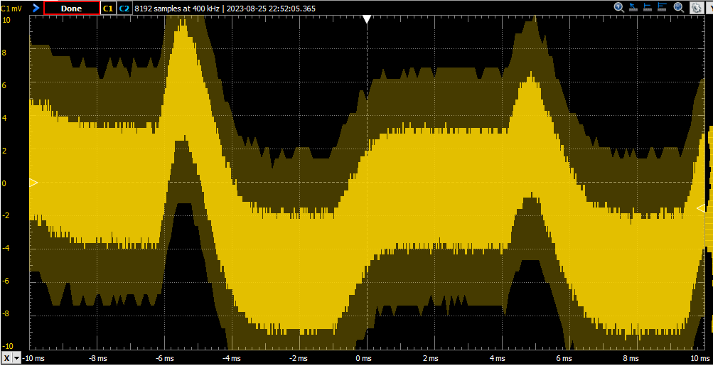
This graph has a different time scale as the previous one (2ms/div vs 5us/div previously). The thick yellow line represents the 12Vp-p ripples, but in addition, a slower undulation due to the set-point adjustment is observed, bringing the total noise to ~20V peak-to-peak.
The regulation is provided by a PID regulator. The PID constants (or gains) Kp, Ki, and Kd can be adjusted by the user depending on their application. Tuning a PID is always a trade-off between speed (how fast the output adjusts to changes of set-point or perturbations), and overshoot. Keeping dielectric elastomer actuators as the default application, overshoot should be avoided at all costs to avoid dielectric breakdown. Consequently, the default PID values are chosen to avoid overshoots, at the cost of a slightly slower dynamics.

The figure above shows how the output adjusts to a change of set point from 0 V to 20%, 40%, 60%, 80%, and 100% of full scale on a 4kV hvps-x. No overshoot is observed, and the rise time is less than 90 ms over the whole voltage range. PID parameters can be adjusted by the user.
Switching mode
The switching mode (SwMode in the python library) refers to the state of the high-voltage output switch implemented with 2 high-voltage optocouplers. To understand the different settings, let’s take a closer look at the hardware output stage.

The optocouplers can be represented as 2 switches in series between the high voltage produced by the converter and ground (for a unipolar hvps-x). The output of the hvps-x is located between the 2 switches. There is a resistor between the output and ground that represents the output voltage monitoring circuit. Representing the optocouplers as switches is a simplification for the sake of the explanations below; a more accurate model would be current sources of 100uA.
The switching mode defines the state of the two switches, which in turn defines the state of the hvps-x output. Here are the different settings you can use:
Off
In off mode, both switches are open. The output is connected to ground through the voltage monitoring circuit. This ensures that if a charged capacitive load is connected to the output it will be quickly discharged and won’t be left at high voltage with the risk of electric shock when touching the device under test. R has a value of 250 MOhm. For a 1 nF capacitive load, the discharge time constant would be 0.25 s. In off mode, no current flows through the optocouplers, and it is recommended to leave the HVPS in off mode when not in used. When the High Voltage safetwy switch (2) is on position ‘0’, the hvps-x switches to off mode.
Low
In low mode, the lower switch is closed, which connects the output to ground (for a unipolar hvps-x). Although the end result is the same as off (0 V at the output), the discharge is much faster. In the future bipolar configuration, the low side of the switch will be connected to a negative voltage instead of ground. As a visual indication that the output switch is in low mode, a blue LED is turned on.
High
In high mode, the high-side switch is closed effectively connecting the output to the output of the HV DC-DC converter, and the voltage produced by the converter will be present at the output of the hvps-x. As a visual indication that the output switch is in low mode, a red LED is turned on
Switching
In switching mode, the state of the two switches swaps between Low and High modes at regular intervals, thus producing a square wave output with sharp transitions. There are two user-settable parameters associated with the switching mode: frequency and duty cycle.

- The frequency f can be set between 1 mHz and 1kHz. Be mindful that when using high frequency values, the waveform shape will depend on the capacitance of the load (refer to Frequency capabilities).
- The duty cycle D can be set between 0 and 1 and represents the fraction of the time the output is high with respect to the period of the signal. A duty cycle of 0.5 means that the output is high for 50% of the period and low for 50% of the period. With respect to the above illustration, D=thigh/T.
Waveform
In waveform mode, arbitrary waveforms can be produced. Waveforms can be defined by parameterising common functions such as sine, triangle, and trapezoid, or using a list of points from a file. The maximum frequency at which waveforms can be produced depend on the load connected to the output (refer to Frequency capabilities).

Switching source
The switching source (SwSrc in the python library) describes what controls the state of the high voltage switches (i.e. the switching mode, described above).
Button
There are two push button on the board. The button controlling the output switches is called S2. The other push button (S3) is used to upgrade the microcontroller’s firmware.
When the switching source is set to button, the onboard push button is controlling the state of the output switches. There are two configuration parameters associated with the button:
- latching or non-latching mode. In non-latching mode, the button is active as long as your press on it, and is inactive when you release the button. Think of the horn of your car. In latching mode, the button changes between activated and inactivated modes each time you press and release it. Think of the on/off button of an appliance, that you press once (and release) to turn on, and press a second time to turn off.
- off state mode. This defines which of the two switching modes (see above section), ‘Off’ or ‘Low’ is used when the button is in its inactive state. Note that for a unipolar hvps-x, this doesn’t make much difference as the output will be 0V for both settings.
When button is used as switching source, the output of the hvps-x takes the following state:
- When the button is inactive, the output state is ‘Off’ or ‘Low’ depending on the off state mode configuration. For a unipolar hvps-x, this means oV at the output.
- When the button is active, the hvps-x output will be set to the currently selected switching mode. The following points should be kept in mind
- For a unipolar hvps-x, using the button as its switching source, the only switching modes that make sense are ‘High’ (the hvps-x outputs a DC voltage when the button is active), or ‘Switching’ (the hvps-x outputs a square wave of frequency f and duty cycle D)
- The user needs to keep in mind that when button is used as a switching source, the switching mode currently selected by the user is only effectively used by the hvps-x when the button is active. Users might wonder why there is no high voltage at the output when a non-zero voltage set point has been defined, and the switching mode is set to high (or switching). The button needs to be activated for the selected switching mode to be applied.
Timer
Timer switching source is admittedly not the best terminology, but we kept it from the original shvps. What it means is simply that the output of the hvps-x is directly controlled by the firmware, and that the button is ignore. The switching mode that the user selects will be directly applied to the optocouplers. When you want to control the switching mode through the GUI or python-library, and don’t care about user-input on the button, then you should use timer as switching source.