This page describes the assembly of the high-voltage components for the most recent revision of the PCBA. For the previous version (1.2/1.3), refer to this page.
Once the low-voltage part of the board is working as expected, it is time to assemble the high voltage side of the board.
EMI shielding of the DC/DC converter
The high-voltage DC-DC converter emits a lot of noise. This noise radiates to the surrounding components and affects the voltage reading circuit. It may also affects other sensitive analogue measurement instruments that you may have in close proximity of the power supply. Commercial power supplies solve this issue by using grounded metallic cases to host the electronics. Most likely, you will use the hvps-x without an enclosure, or maybe a 3D-printed or laser-cut enclosure made of plastic. Although not 100% necessary (the firmware filters the voltage reading to remove the induced noise), we strongly recommend to shield the high-voltage DC-DC converter prior to soldering on the board. You will improve the performance of the voltage feedback reading circuit, and your hvps-x won’t radiate noise in the lab.
The BOM lists a roll of copper tape. The issue is that it is quite pricy and you will only need about 40cm from a 5m roll. But if you have other metallic tape it will work too, a thick aluminium foil etc.

The picture above shows a DC-DC converter wrapped in the copper tape listed in the BOM. The front pins are the low voltage power pints. We have put some kapton tape (any insulating tape will do) to prevent electrical contact between the tape and the pins, or the pads on the PCB. The pin at the back on the right is ground, and it can therefore touch the copper (however it doesn’t have to; we’ll connect the shield separately to make sure we have a good contact). The pin on left is the high-voltage output. Kapton tape has been added to increase insulation, and copper has also been partially removed on the side:
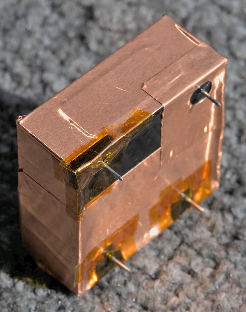
You want to cover as much of the surface as possible with tape, but must make sure to provide enough clearance and creepage distance between the high voltage terminal and ground to avoid the risk of leakage and sparks.

Soldering the high-voltage components
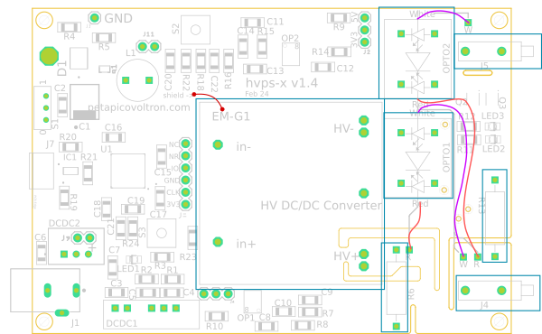
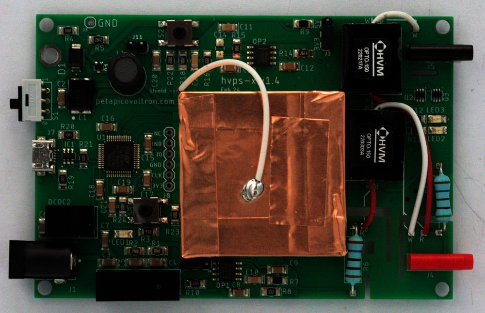
- Solder the optocouplers OPTO1 and OPTO2. The silkscreen has marking “red” and “white” to indicate the orientation of the optocouplers according to the colour of the wire sticking from the device’s case. The illustration above shows where the white and red wire of each optocoupler must be connected (see also photo below). The white wire is coloured in magenta in the schema above to be visible. The pads to which the wires must be soldered are indicated with the letter R/W referring to the white and red wires. You need to cut the wires to the correct length to reach the pad to which they need to be soldered and remove the insulation at the end. The wire length should be adjusted so that they reach the pads when the optocouplers are inserted without being too long. It’s better to start too long and shorten if required!
- Solder Resistors R6 and R13. They don’t have the same value, so don’t mix them (refer to BOM). When you solder these two resistors, make sure to keep the resistor’s body ~5 mm above the board. This is to ensure that no flux residues (or dust) gets trapped between the resistor and the board.)
- Solder connectors J4 and J5. J4 is the live connector and should be red. J5 is the ground connector and should be black (see picture below). In case you have also assembled previous versions of the board, take note that the red/black connectors have been swapped on this version.
- Solder the DC/DC converter EM-G1
- Solder a wire between the HV DC/DC copper EMI shield and the ground pad labelled shield at the top left corner of the converter, as shown on the illustration above. If you used aluminium for the shield, you will not be able to solder the wire to the shield. You can use some conductive tape or glue to fix the wire to the shield. Make sure you have good electrical contact by measuring the resistance between the shield and ground. It should be <1 Ohm.
- On the backside of the board, cut the excess leads of the resistors, and the excess red and white wires from the optocouplers.
Once you have finished placing these components, make sure to clean the board from flux residues, especially in the high-voltage section of the board. Flux residue (or other contamination) can drastically reduce the breakdown strength of the board and lead to damages when the high voltage is applied.
Next step: Test the high voltage components and potting!