A new PCBA version, version 1.4 has been released and documented on the website. This is the version we recommend to make. It includes 2 output current settings, a pad to connect the ground plane to earth ground for increased safety, and general routing improvements. We have also released a new 3D-printed protection enclosure for PCBA v1.4, which includes LED pipes, a physical button, and an access on the side to the grounding pad.
Current setting

With PCBA v1.4, the output current of the optocoupler can be changed between normal current output (~100 μA) and high current output (~200 μA). High current mode is useful if working with large actuators (i.e. large capacitances), and / or if actuation at higher frequency is required. Normal current setting is obtained if jumper J2 is positioned at the bottom (as on the image above), indicated by marking 3V3 on the silkscreen. If the jumper is placed at the top position (marking 5V), the output will be in high current mode. We recommend using normal current whenever possible for increased safety.
The oscilloscope screen captures below illustrate the effect of changing from normal current to high current mode. A 1.4 nF capacitor is connected to the output of the hvps-x in all the tests below, to emulate a large dielectric elastomer actuator.

The hvps-x was set in switching mode at 2Hz, and the rising edge of the signal was measured with a high-voltage probe (probe capacitance negligible compared to the 1.4nF capacitor). As seen on the screen capture above, the output voltage increases by 1137 V in 15 ms. The calculated output current (given that the load is a 1.4nF capacitor) is 106 μA.

the graph above shows the whole waveform. Note that as the voltage increases, more current leaks through the high voltage probe (100 MΩ impedance). at 6kV, 60 μA is wasted in the probe, i.e. 60% of the current, hence why dV/dt reduces when the voltage increases. When the hvpx-x is used without the high-voltage probe, charging of a 1.4 nF capacitor is faster. If the rate of 76V/ms remains constant during the whole charging portion of the curve, it will take 79 ms to charge to 6kV, while it takes about 150 ms with the probe.
The jumper is now changed to high current mode.

As seen on the screen capture above, the output voltage in high current mode increases by 2066 V in 15 ms. The calculated output current (given that the load is a 1.4nF capacitor) is 193 μA, i.e. about twice the output current of the normal mode.

More current available means shorter rise/fall time, which is especially useful when driving larger capacitive loads.
Grounding tab
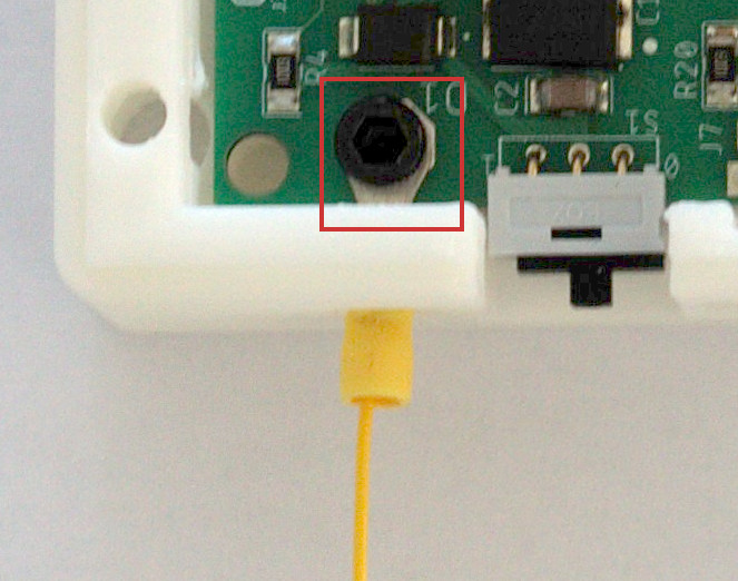
For increased safety, we recommend to connect the hvps-x ground plane to earth ground. V1.4 of the PCBA renders this easy by providing a ground pad near the edge of the board. The enclosure was modified to add a hole below that bad and an opening in the side of the box. A ring terminal can then be screwed to the PCBA and enclosure, with the wire going through an opening in the box. The other extremity of the wire can be connected to an earth ground connection on your lab work bench.
hvps-x should be operated with this connection connected to earth ground. This is especially important if you are using a laptop to control the hvps-x. In this configuration, the USB shield is not necessarily grounded. The AC-DC power adapter is also insulated, hence not providing a direct connection between the hvps-x and earth ground.
Enclosure
The protection enclosure for PCBA v1.4 now includes LED pipes to better guide the light from the board-mounted LED to the top of the box. It also includes a friendly physical button on the top side to turn the output on/off (if button mode selected in the GUI).
